Absolute workhorse of RF switching.
WHAT IS A PIN DIODE?
A PIN diode is a semiconductor diode with three layers:
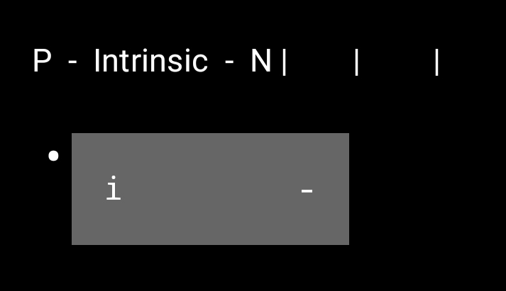
The middle layer is a thick, undoped (intrinsic) region.
That middle layer is the magic.
WHY IT’S DIFFERENT FROM A NORMAL DIODE
A normal PN diode is mainly for rectifying (one-way conduction).
A PIN diode is designed to act like:
- A current-controlled resistor at RF
- An RF switch
- An RF attenuator
It behaves very differently at high frequency.
HOW IT WORKS (RF VIEW)
When forward biased:
Current flows Charge fills the intrinsic region The diode behaves like a LOW RESISTANCE (few ohms) RF passes through
When reverse biased (or zero bias):
No stored charge Very high resistance (kilo-ohms) RF is blocked
So instead of acting like a rectifier, it acts like a controllable RF resistor.
WHY THE INTRINSIC LAYER MATTERS
The thick intrinsic region:
- Increases carrier lifetime
- Makes the device behave resistively at RF
- Prevents it from acting like a simple detector
At RF, we don’t want rectification. We want a controllable impedance.
That’s what the PIN structure gives us.
WHY RADIO ASTRONOMERS LOVE THEM
They are:
- Fast (nanoseconds to microseconds)
- No moving parts
- Low distortion
- Long lifetime
- Compact
Perfect for:
- Dicke switches
- T/R switching
- Step attenuators
- Phase shifters
SIMPLE RF SWITCH EXAMPLE
Series switch:
RF in —- PIN —- RF out | Bias
Forward bias: Low resistance -> signal passes
Reverse bias: High resistance -> signal blocked
Shunt switch:
RF line —-+—— RF out | PIN | Ground
Forward bias: Shorts RF to ground
Reverse bias: Leaves line open
Many designs combine series + shunt for high isolation.
AT 1420 MHz (Hydrogen Line)
Typical small-signal RF PIN diode:
On resistance: 2 to 10 ohms Off capacitance: 0.1 to 0.5 pF Isolation at 1.4 GHz: very usable
Much faster and quieter than a relay.
MENTAL MODEL
Think of a PIN diode as:
“A resistor whose value is controlled by DC current, but only for RF.”
That’s the intuition.