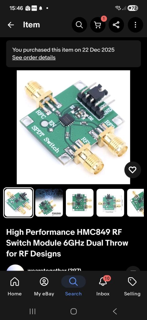
The HMC849 is a high isolation, non-reflective DC to 6 GHz SPDT (Single-Pole, Double-Throw) RF switch available in a 16-pin, 4×4 mm LFCSP surface-mount package.
Data Sheet:
https://www.astronomy.me.uk/wp-content/uploads/2026/01/Analog-Devices-HMC849a-data-sheet.pdf
Key Pin Descriptions:
The specific pinout details require referencing the official Analog Devices datasheet, but the key connections are as follows:
VDD: This is the single positive supply voltage input, typically ranging from 3V to 5V.
GND: The ground connection for the device, including the exposed pad on the bottom of the package which must be soldered to the PCB ground plane for proper thermal and electrical performance.
RFC: The common RF port (RF Choke). This is the input that is switched between the two output paths.
RF1 & RF2: The two RF output ports. The control pins determine which of these ports the RFC signal is routed to.
VCTL (Control Voltages): The switch operates with CMOS-/TTL-compatible control logic. The control pins accept 0V or VDD.
EN (Enable): An enable input pin. Setting this to a logic high (“all off” state) puts the switch into a high isolation state where neither RF1 nor RF2 is connected to RFC, and the input is internally terminated.
Control Logic The switch status is controlled by the voltage applied to the control pins.
| VCTL Input | Switch Status |
| Logic Low (0V) | RFC connected to RF1, RF2 isolated |
| Logic High (VDD) | RFC connected to RF2, RF1 isolated |
For the precise pin number mapping for each of these functions, please consult the official HMC849A Datasheet on Analog.com.