Alex many thanks.
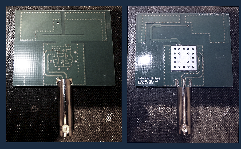
Wow — seeing the actual copper patterns on the other side of the board completely changes the picture. This isn’t a simple folded‑dipole board at all; it’s a genuinely sophisticated microwave feed. The asymmetric ground plane, the via‑coupled parasitic structures, and the shaped planar radiator make it clear that this design is operating at a much higher level than I first assumed.
The LNA input broadband “fat” planar radiator is almost certainly doing the real radiating, and the LNA input is almost certainly coupled at a low‑current, high RF potential node. That kind of weak coupling stabilizes the impedance and preserves the wide bandwidth the designer was aiming for. No wonder the matching network on the opposite side looked like something meant for a high‑impedance source — that’s exactly what it is.
And as Don pointed out, the external metal piece isn’t a multi‑element folded dipole at all — it’s a shaped near‑field reflector that completes the beam‑forming illumination environment for the PCB radiator. When you put all of this together, plus whatever careful RF work likely went into the LNA under the shield, it’s easy to understand why people say this is the such a good hydrogen‑line feed that they’ve used on a dish. The whole thing is remarkably compact for how much engineering is packed into it.
Thank you
Adrian
From Alex:
Photos of both Sides of KrakenRF Discover H-Line feed PCB: